

SK Hynix Market Position and Growth
- SK Hynix is currently undertaking the world's largest memory buildout, producing the majority of the global supply of high-bandwidth memory (HBM) chips essential for artificial intelligence 0s.
- The company recently debuted on the Nasdaq in a $26 billion listing, marking the largest foreign listing in the exchange's history 25s.
- High demand for HBM from major technology firms like Nvidia and Apple has created significant scarcity, leading to long-term supply contracts and rising prices for consumer electronics 35s.
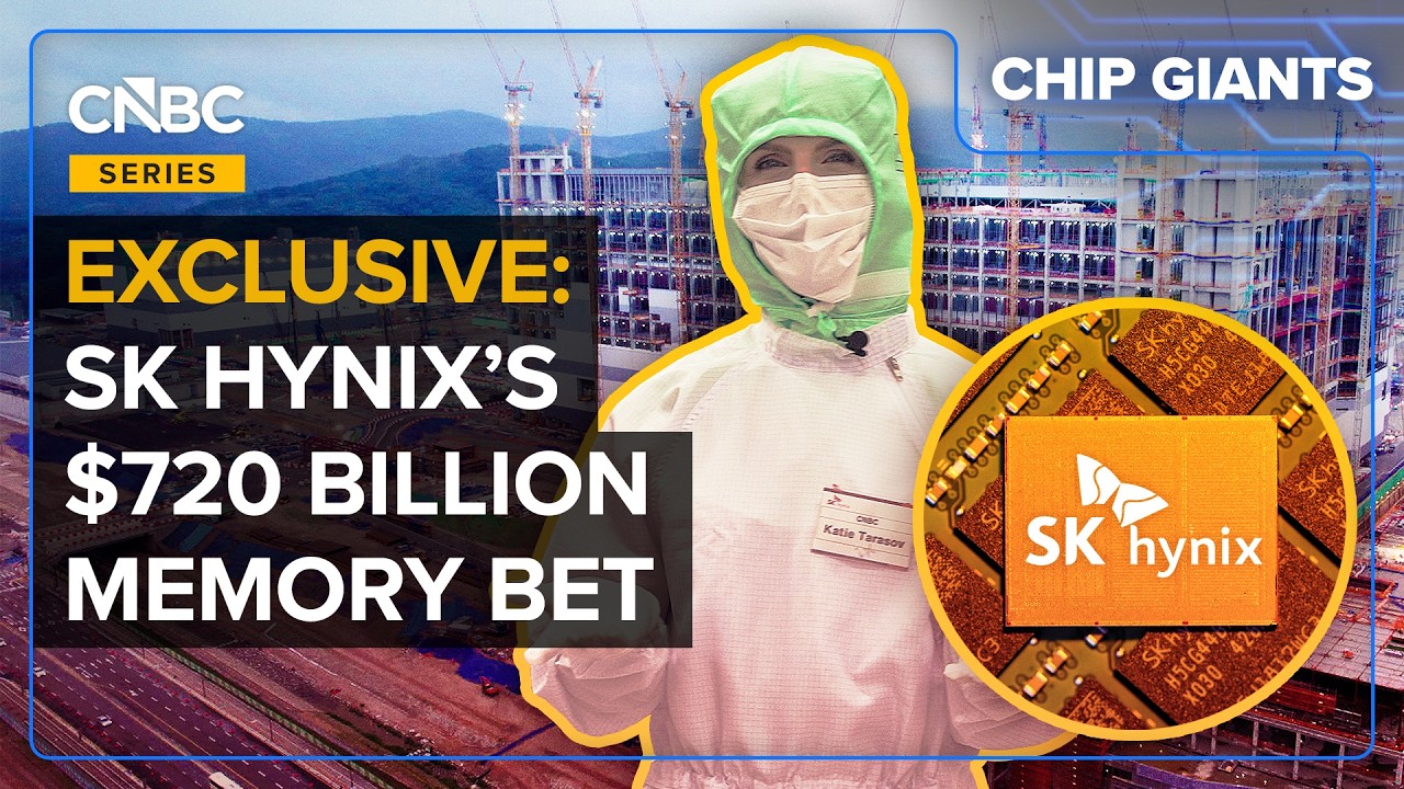
- SK Hynix plans to invest $720 billion to triple its production capacity by 2034, though the company acknowledges the inherent risks of the cyclical "boom and bust" nature of the memory industry 55s.
Corporate History and Evolution
- The company originated as the Sunkyong Textile Company, founded by the uncle of current Chairman Chey Tae-won, and later diversified into sectors including petroleum and telecommunications 1m35s.
- In 2012, SK Group acquired Hynix Semiconductor—a firm formed from the chip divisions of Hyundai and LG—for $3 billion, subsequently rebranding it as SK Hynix 1m55s.
- SK Hynix developed the world's first HBM in 2013, despite the lack of immediate commercial applications at the time 2m5s.
- The company achieved its first commercial HBM sale in 2015 for AMD Radeon graphics cards, and began seeing significant returns around 2017 due to demand from Bitcoin miners 2m20s.
Competitive Landscape and Market Leadership
- While Samsung began HBM production in 2015 and served as Nvidia's original supplier, SK Hynix became Nvidia's primary supplier after being the first to produce HBM3 following the rise of ChatGPT in 2022 2m35s.
- SK Hynix is currently the market share leader in HBM and serves as the largest asset within the SK Group, which consists of over 100 subsidiaries 2m55s.
- The company's stock rose 13% on its first day of U.S. trading, reflecting strong investor interest 3m15s.
- While the memory industry offers potential for significant long-term profits, the Korean market remains highly volatile, and recent gains have faced downward pressure amid broader instability in chip stocks 3m30s.
Yongin Cluster Infrastructure Development
- SK Hynix is currently undertaking the largest memory fabrication buildout in its history, centered at the Yongin cluster in South Korea. 0s
- The Yongin cluster spans 45 million square feet, an area roughly equivalent to 600 soccer fields, and is designed to house four fabs, with the first featuring six clean rooms. 3s
- Construction at the Yongin site began in 2023, with the first fab scheduled to open in February and the entire complex projected to cost approximately $400 billion. 13s
- Due to South Korea's limited land availability and mountainous terrain, which covers 70% of the country, the Yongin fab is being built vertically rather than sprawling outward, requiring the flattening of mountains. 22s
Government Support and Industry Demand
- The South Korean government is supporting the infrastructure needs at Yongin through a chip support package worth up to $22 billion. 35s
- In June, the South Korean government unveiled a broader plan to double the country's memory production within five years, which includes new mega fabs from Samsung and a future SK Hynix cluster in the southwest. 42s
- Major technology companies, including Microsoft, Meta, Amazon, Nvidia, and AMD, are actively engaging with Korean manufacturers to secure supply contracts, leading to high demand for local hotel accommodations. 52s
- Executives such as AMD’s Lisa Su and Nvidia’s Jensen Huang have visited Korea to meet with memory suppliers, with Huang explicitly requesting increased production from SK Hynix. 1m5s
- High memory costs and supply shortages have impacted major companies, with Amazon increasing its 2026 capital expenditure estimate and Apple citing memory constraints as a factor in its weak guidance and increased product pricing. 1m25s
Technological Challenges and HBM Architecture
- The scarcity of memory has encouraged the rise of new chip companies like D-Matrix, Groq, and Cerebras, which utilize alternative architectures to reduce reliance on DRAM. 1m45s
- Nvidia is reportedly testing lower-memory versions of its next-generation GPUs, a move that could potentially decrease the industry's appetite for High-Bandwidth Memory (HBM). 1m55s
- To address record-high customer pressure, SK Hynix has accelerated its construction timeline, now targeting the completion of the fourth fab by 2033, which is 12 years ahead of the original schedule. 2m6s
- SK Hynix dominates the market for HBM, which consists of stacked DRAM chips that enable rapid data access for processors and AI accelerators. 2m15s
- The "memory wall" refers to a situation where even the fastest processors are limited by the speed at which data can be processed and accessed. 2m28s
- Achieving higher HBM performance requires complex packaging, where up to 16 DRAM chips are stacked and connected. 2m35s
Manufacturing Facilities and Advanced Packaging
- SK Hynix opened the $13 billion M15X fab in Cheongju in 2025, a facility described as being as tall as a 33-floor apartment building. 2m45s
- SK Hynix operates a production facility with a footprint equivalent to 13 football fields, where it manufactures HBM3E and HBM4 memory products 0s.
- The production of HBM4 involves over 1,000 process steps and requires approximately four months to complete 12s.
- SK Hynix utilizes a proprietary packaging technology called MR-MUF, which was developed around 2019 to regain a competitive edge in the HBM market 22s.
- MR-MUF is a low-pressure method that bonds all DRAM chip layers simultaneously and injects a protective liquid between them to reduce heat and warpage, resulting in stacks that are 40% thinner 33s.
Supply Chain Dynamics and Future Product Development
- While HBM stacks historically generate higher revenue per wafer than conventional DRAM, Samsung remains the market share leader in standard DRAM and NAND Flash 53s.
- SK Hynix is investing $67 billion to construct two new fabs, one dedicated to NAND Flash and another to packaging, to support the supply chain before components are sent to TSMC for integration with logic chips 1m12s.
- Packaging at TSMC has become a bottleneck due to Nvidia reserving a significant portion of TSMC's advanced capacity 1m23s.
- Although SK Hynix is considered the leader in HBM, some industry observers suggest Samsung is catching up and may be ahead in HBM4 for the Rubin architecture, though SK Hynix maintains superior manufacturing cost efficiency and operating margins 1m35s.
- The HBM4E enhanced product contains 380 billion transistors 2m0s.
- Future HBM5 development is shifting toward customer-oriented, custom designs co-developed with specific AI processors for clients like Nvidia and Google 2m8s.
Strategic Partnerships and Premium Pricing
- The transition to custom HBM is intended to help SK Hynix mitigate the traditional boom-and-bust cycles associated with the memory industry 2m35s.
- Memory contracts have evolved from one-year terms to five-year agreements, with SK Hynix reporting ten long-term agreements involving $10 billion in prepayments 2m45s.
- Nvidia has secured a stable HBM supply and agreed to co-develop next-generation memory as part of a $500 billion deal with SK Group, which also includes the construction of data centers by 2027 3m10s.
- HBM is shifting memory from a low-margin commodity to a premium product with bespoke pricing, which has contributed to an 80% increase in smartphone DRAM prices since the previous quarter 3m30s.
- The high cost of production is driven by expensive equipment, such as overhead hoist transports, which cost $70,000 each; the facility currently utilizes 700 of these units 4m0s.
Advanced Lithography and Industry Cycles
- The SK Hynix headquarters in Icheon, located southeast of Seoul, houses the company's largest production facility and features what is described as the world's longest clean room track for transporting wafers between fabs 0s.
- The facility utilizes extreme ultraviolet (EUV) lithography machines from ASML to etch microscopic circuitry onto chips, including the memory industry's first installation of ASML's most advanced $400 million high-end model 18s.
- SK Hynix plans to invest up to $8 billion in EUV machines by 2027, and South Korea currently represents ASML's largest market, accounting for 43% of its sales 35s.
- The total projected expenditure of $720 billion for these fabrication facilities is more than 18 times the $39 billion allocated by the U.S. government for chip manufacturing incentives under the CHIPS Act 45s.
- While the memory industry has historically operated on a boom and bust cycle, the current AI era is viewed as a structural change that may lead to a longer cycle, with analysts predicting demand will outstrip supply until at least 2030 1m0s.
Market Risks and Financial History
- Potential market risks include a future supply glut once additional fabs from competitors like Micron and Samsung become operational 1m25s.
- SK Hynix previously faced significant financial challenges, including near-bankruptcy during the Asian financial crisis of the late 1990s and an operating loss of nearly $6 billion during the 2023 memory oversupply downturn 1m35s.
- AI development presents resource challenges, including high consumption of energy, materials, silicon, and water, though it is also viewed as a potential tool to reduce human labor requirements 1m50s.
- Building AI infrastructure in the U.S. is considered more expensive than in Korea due to higher costs for land, electricity, water, and regulatory requirements, with the cost of building a fab in Korea estimated at half that of the U.S. 2m20s.
U.S. Expansion and Indiana Facility
- SK Hynix is constructing its first U.S. facility in West Lafayette, Indiana, which is an advanced packaging plant rather than a front-end production fab, representing a $4 billion investment 2m45s.
- The 133-acre Indiana site, which began groundbreaking in April 2024, will include a fab and R&D centers, with plans to create approximately 1,000 long-term jobs 3m5s.
- The Indiana project is supported by over $1 billion in incentives, including $458 million in federal CHIPS Act funds and a conditional package from the state of Indiana valued at more than $700 million 3m35s.
- Indiana was selected for the facility due to its availability of power and water, government support, and proximity to Purdue University and the University of Illinois Urbana-Champaign for manpower 3m20s.
- Despite the new U.S. facility, SK Hynix will continue to manufacture its memory chips in Korea and at three existing fabs in China 3m50s.
International Trade and Global Strategy
- Due to U.S. export controls, SK Hynix and other companies are prohibited from selling their most advanced High Bandwidth Memory (HBM) products in China. 0s
- China is developing its own domestic manufacturers for AI-related memory and is advancing rapidly in this sector. 5s
- Samsung is establishing a large fabrication plant in Texas, though the facility is dedicated to logic chips rather than memory. 22s
- Micron is investing $250 billion into memory manufacturing facilities located in Idaho and upstate New York, a project expected to create 100,000 American jobs. 28s
- The U.S. Commerce Secretary has publicly encouraged SK Hynix and Samsung to build memory manufacturing facilities within the United States. 42s
- SK Hynix has expressed a willingness to build facilities in the U.S. but faces challenges in identifying suitable locations. 50s
Intel Acquisition and Future Outlook
- In July, SK Hynix officially denied reports from Korean media suggesting the company intended to acquire Intel’s ongoing fabrication project in Ohio. 56s
- SK Hynix acquired Intel’s NAND and SSD business for $9 billion in 2021, forming the subsidiary Solidigm and becoming the world's second-largest NAND producer. 1m5s
- In January, SK Hynix restructured Solidigm to launch a $10 billion AI-focused company in the United States. 1m15s
- The strategy behind the new U.S.-based AI company is to combine American software engineering expertise with the hardware manufacturing strengths found in Korea, Taiwan, and Japan. 1m20s
- SK Hynix plans to begin packaging chips at a facility in Indiana by 2028. 1m38s
- The first clean room at the Yongin cluster in Korea is scheduled to begin memory production by February. 1m43s
- The memory shortage is projected to reach its most severe point in the coming year. 1m48s
- SK Hynix aims to defend and expand the memory market as rapidly as possible. 1m52s